64-CHANNELs SiPM IMAGING MODULE

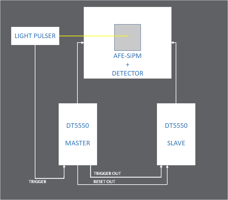
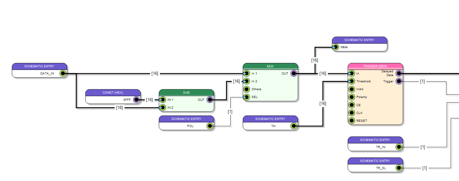
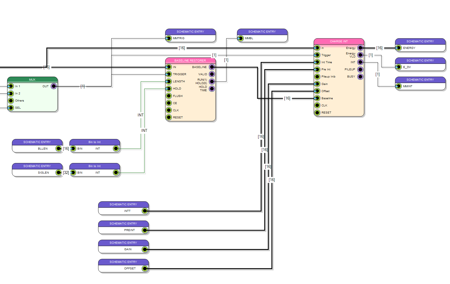
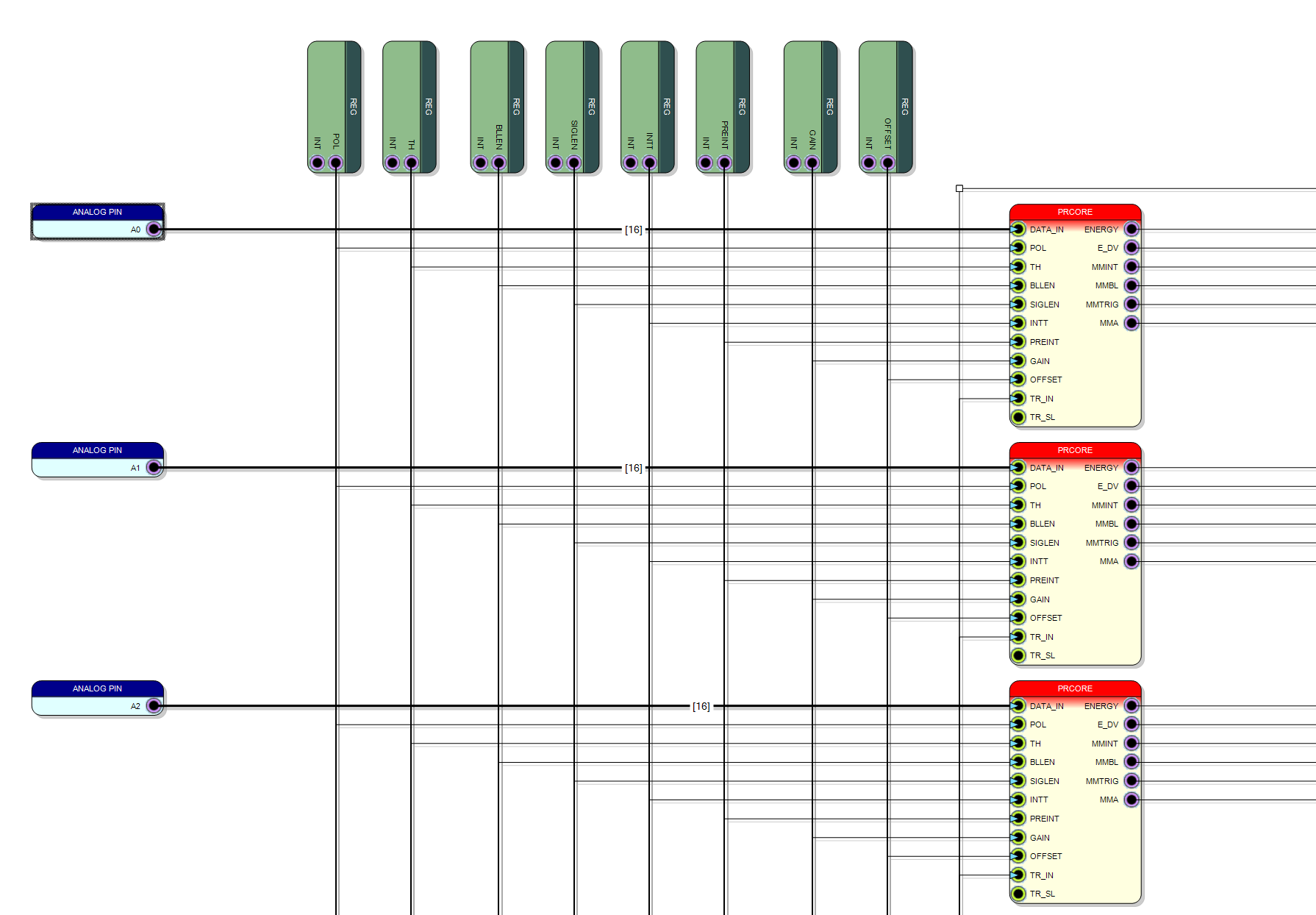
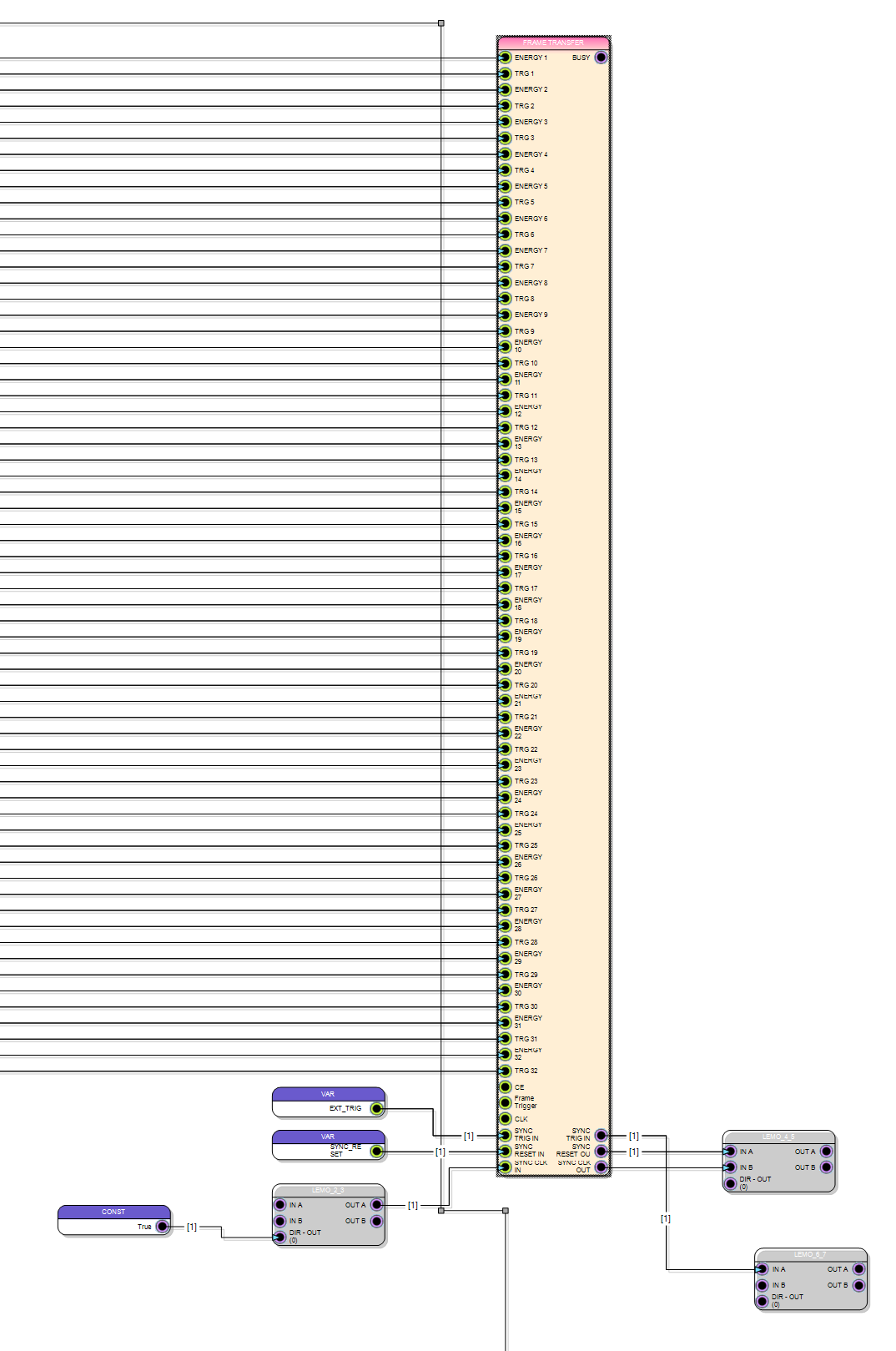
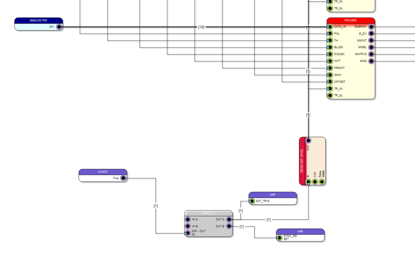
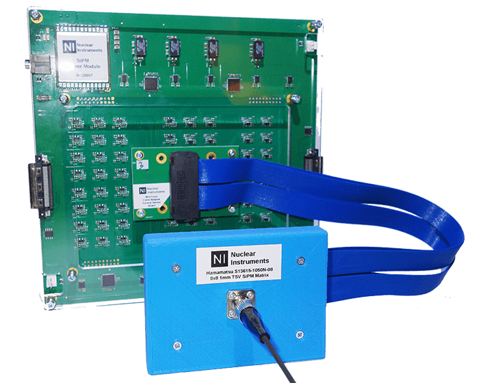
The DT5550-AFEs board is outstanding readout system that, in conjunction with two DT5550 allows the readout of up to 64 independent SiPM channels making the solution ideal for SiPM matrix in imaging and spectroscopy application. n conjunction with two DT5550, the DT5550AFEs allows the direct sampling of the analog signal generated by the SiPM in order to process it with user programmable digital pulse processing filter. This application note shows how to develop a firmware to acquire the waveform, and calculate the energy spectrum in realtime using charge integration

SETUP OVERVIEW

The readout system require the usage of two digitaizer DT5550. The digitizer operates at 80 MSPS/14 bits with 32 channels each one The firmware for the two board is the same. The two board are connected by two syncronization lanes: common trigger and common reset in order to capture syncronous data and be able to recostruct images on the PC side. One of the board works as master, generating the common trigger and the reset signal. The second board works as slave, triggered by the master board Syncronization is done by the assumption that the two board are able to count the number of events without loosing any. The common reset generates a syncronous T0 reference. Offline, the data from the two board are merged and syncronized using the event counter id. A second syncronization mechanism based on a common timecode is also available

FIRMWARE OVERVIEW

The firmware diagram is composed by 5 blocks

  • 32 Processing Units that contains: trigger, baseline restorer, charge integrator
  • Frame transfer module: create 32 pixel image and implements the PC communication
  • Oscilloscope: dumps waveform and transfer it to the control PC
  • External trigger logic and Syncronization
  • Memory mapped I2C transfer controller to configure HV generator

PROCESSING CORE

The following diagram shows the processing core. Several virtual instruments are involved in the processing chain:

  • Signal inversion to accept both positive and negative polarity signals
  • Derivative trigger with programmable treshold
  • Baseline restorer based on programmable length moving average
  • Charge integration with configurable integration time and pile up rejection logic
  • Multipled trigger source (internal/external)

COMPONENT REUSE

The processing block is used 32 times in the design. It iplements a user defined Virtual Instruments and it exports ports (Schematic Entry) that will appear as input/output ports. The configuration parameters are connected to shared memory mapped register that can be configured in real-time by command issued from usb bus. Register and C/C++ library and driver are automatically generated by the scicompiler

IMAGING MODULE

Charge integration block gets in input the 32 energy and triggers from the Processing Units. It assemle the energy value in frame (image) transfering them to the PC. The software shows this information as pixel map (image) and as energy spectrum. The blocks add also timining information and syncronization counter.

EXTERNAL TRIGGER

In order to acept an external trigger, the DT5550 back Lemo connector are used (I/O 0). An edge detector is used in order to detect only the rising edge of the trigger signal.

SDK - LIBRARY GENERATION

SCICompiler generate in output

  • The FPGA firmware as bitstream and DT5550 upgrade file
  • VHDL code. (some of the IP are encrypted)
  • Drivers for Windows and Linux (compiled)
  • Library in C/C++ for Windows and Linux (open source), the VC++ project and make file
  • An example application

JSON REGISTER FILE

A JSON file that describe all memory mapped pheripheral, their addresses and their control register. The JSON file can be used to dynamical map register in the firmware or can be imported in Resource Explorer tool to immediately control the behave of all blocks without write any code