Description
Highlighs:
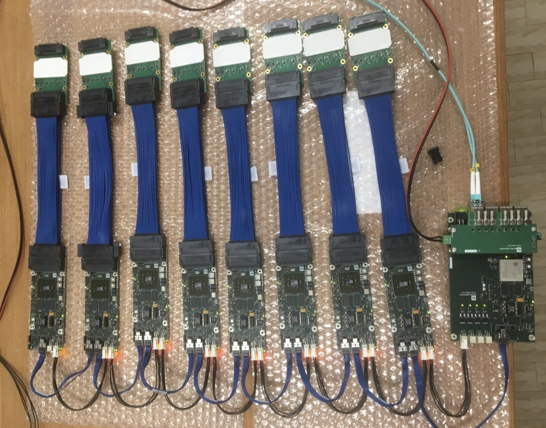
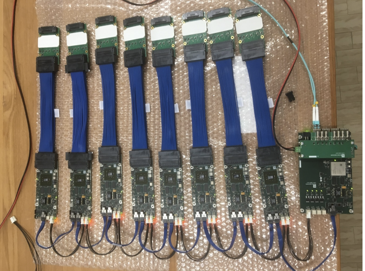
64 pixel indipendently readout per board
Daesy chain solution: up to 126 board per chain
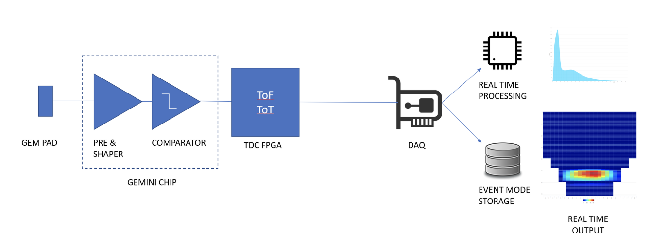
Time over threshold and time of flight measuraments.
64 TDC channels with 0.5 ns resolution
4ns double hit resolution
Up to 100 Mcps per chain
Up to 5 Mcps on single pixel (limited by the ASIC)
10 Gbps optical link per chain
Realtime monitor software with advanced analysys features
List mode data dumping
External (on lemo) and internal T0
External programmable VETO
Single channel programmable VETO
External busy output
PCIE readout board, 8x GEN 3, 40Gbps with realtime data processing in hardware
12V, 1.5 A
Linux server software
Web interface to control and monitor acquisition
Run database with API to interface the server DAQ with existing beam facility software
Software
The software is based on a server side daemon and a client user interface. The acquisition daem runs on a linux server while the client webpage works on any modern broswer allows the configuration of managing of the system. All operation parameters of the ASIC (i.e. channel threashold, gain, veto) and DAQ parameters (like T0 source, T0 frequency, etc) can be configured by this interface.
The software receive data from the FPGA and rencostruct in live, images and histograms. The software is capable to store data on disk in form of list while, at the same time, it perform live data processing.
The software is capable to perform the following online analysys:
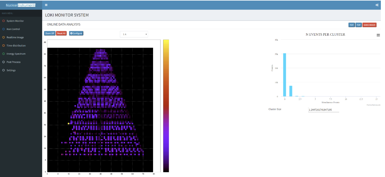
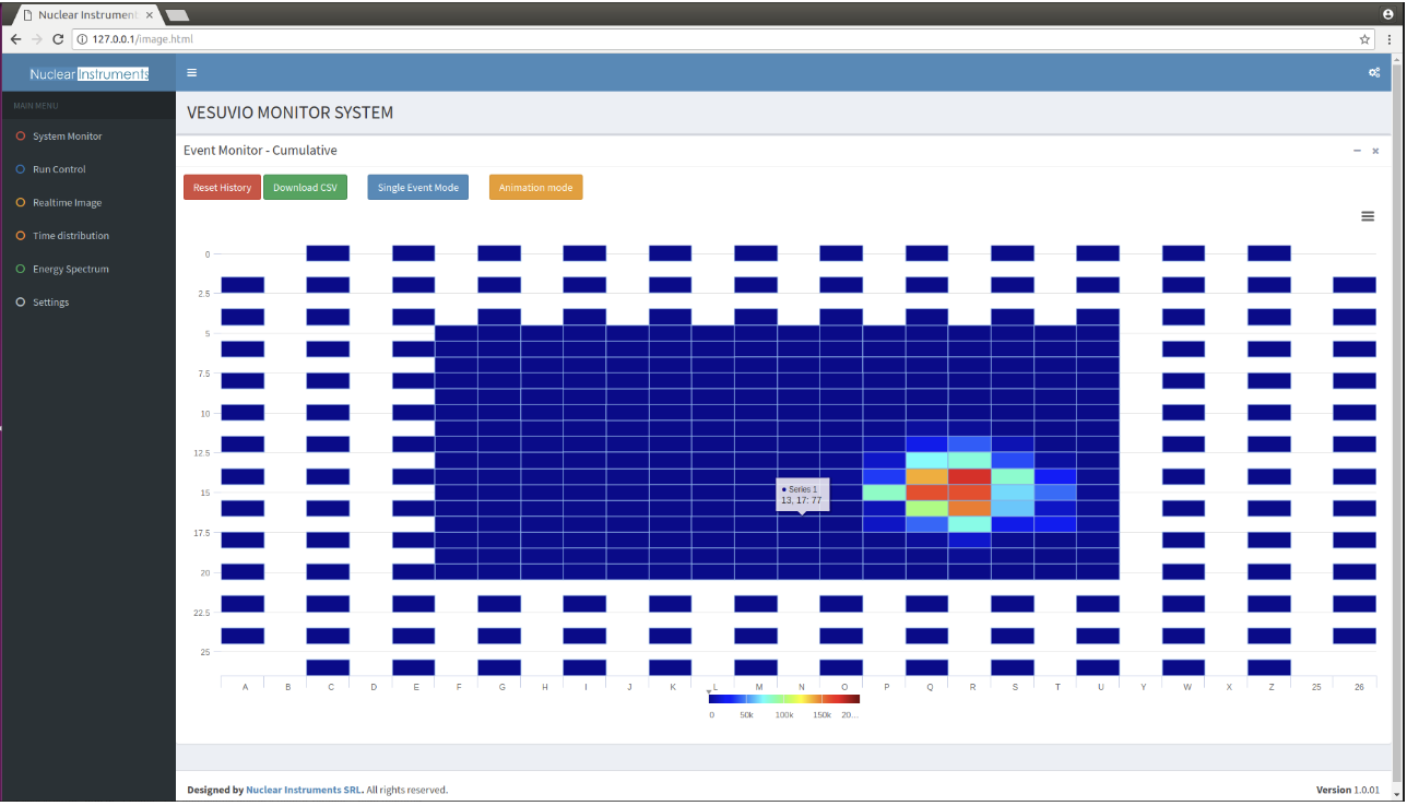
Image recostruction based on the pixel remap matrix that allows to readout any shape detector even if not rectangular
Display integral and realtime counts image
Display integral and realtime ToT image
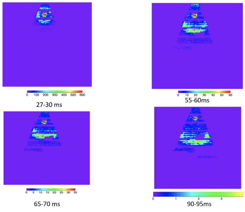
Display images sliced by ToT
Display images slliced by ToF
Display TOF histogram for each channel
Display TOT histogram for each channel
Display TOT/TOF sum histogram applying calibration
Realtime calculation of statistic information like, input rate, T0 rate
The software include a MySQL based run database to store all runs information, including parameters like machine run, run current, type of run, and other custom parameters.
All data are stored server side and raw/processed data can be download via web interface.
An API interface in available to allows users to syncronyze the acquisition/the database with existing facilities software. The acquisition process can be totally controlled via API
The web interface include a slow control monitor that can be configure to collect information like HV status, detector temperature/humidity. It also allows to monitor the status of all boards providing information like link load, FPGA load, input/output rate, deadtime.
ASIC
In principle can be coupled with any asic capable to produce a TOT (time over threshold) LVDS or CMOS signal
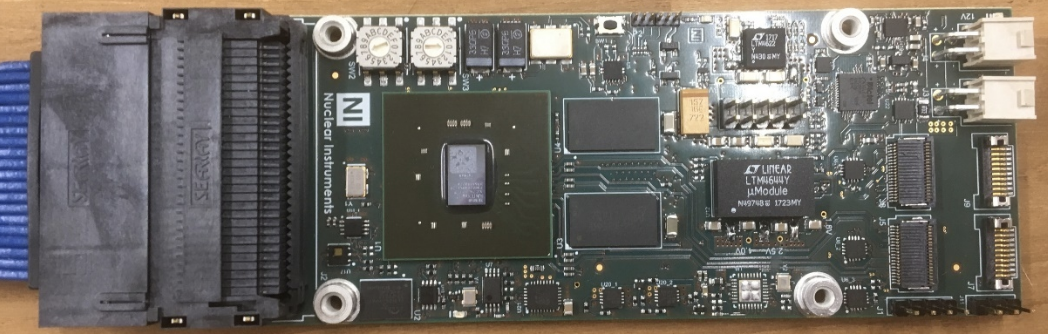
The system is designed to operate with GEMINI ASIC has been developed by the Microelectronic Group at University of Milano-Bicocca in collaboration with the IFP-CNR and the LNF INFN institutions. It has been thought to be dedicated to Triple GEM detector structures, but it can easily be re-adapted for detectors with similar performance. It is made of 16 detecting channels, each including a Charge Sensitive Preamplifier (CSP) with auto-tuned feedback capacitor and a Discriminator with a channel independent programmable threshold. The automatic calibration feature is provided in background by a dedicated unit, able to reach a feedback capacitor resolution less than 5%. The comparator programmable threshold is realized through the inclusion of a 9-bit R-2R Ladder DAC, with 1.2 mV LSB and 500 mV (or externally set) full-scale. The 9-bit threshold digital word can be set through an on-chip I2C interface, with dedicated registers. Two output signals for each channel are generated. The main output is digital. In fact, an LVDS signal is available for event counting rate up to 5 Mcps. In addition, making off-chip spectroscopy measures or checking the detector signal is possible via the analog CSP output.
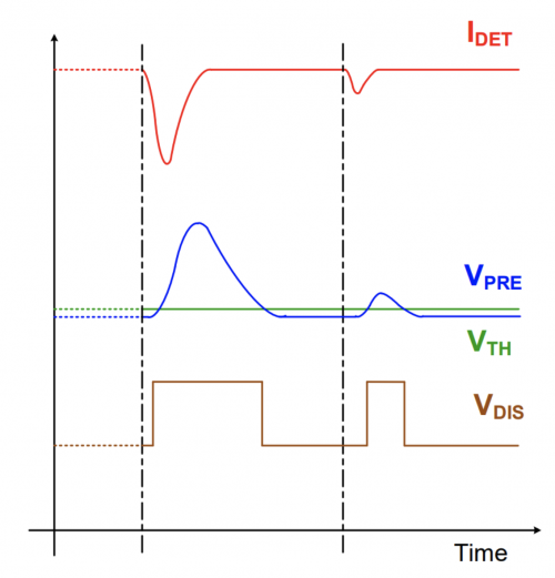
In Figure the GEMINI read-out scheme is depicted, together with a channel main signals example plot. The SoC is made of 16 channels where, with the inclusion of a Charge-Sensitive Preamplifier (CSP), the signal from the detector is converted from charge domain to voltage domain. Then, the Discriminator (DISC) compares the CSP output voltage level with a threshold, set by an R-2R Resistive DAC and specific for each detecting channel, generating the Event Detection output signal. This output is then converted into LVDS standard through a dedicated driver. The channel also produces an analog output signal, which is the buffered CSP output.


The Charge-Sensitive Preamplifier
The CSP composes of a Single Stage Telescopic Operational Amplifier (Opamp) with the CF capacitor and the RF resistor connected in feedback. The Q-V Gain imposed by specifications, i.e. 1 mV/fC, sets directly CF to 1 pF. With a 40 pF CD (pixel capacitance) maximum value, dimensioning the Opamp to obtain 58 dB DC-Gain and 80 µVRMS of in-band integrated noise means that the Signal-to-NoiseRatio lies in a range between 19 dB and 43 dB, with minimum (30 fC) and maximum (500 fC) charge respectively, while the charge collection efficiency is 98%.
The Discriminator
As regards the DISC, the main target is to reduce the input stage offset, in order to achieve the sensitivity and the detection jitter required (3 fC and 9 ns respectively). This means that the maximum tolerated offset is 3 mV after the CSP conversion, as well as for the R-2R Resistive DAC LSB, representing the minimum threshold. Designing the DISC with a mirrored structure and exploiting the inter-digitated layout technique allows to limit the offset within specs. Dealing with the threshold, the 9-bit R-2R Resistive DAC has a 1.2 mV LSB and 500 mV full-scale, set from the external. The input digital words, independent for each channel, are stored into dedicated registers managed from the I2C interface.
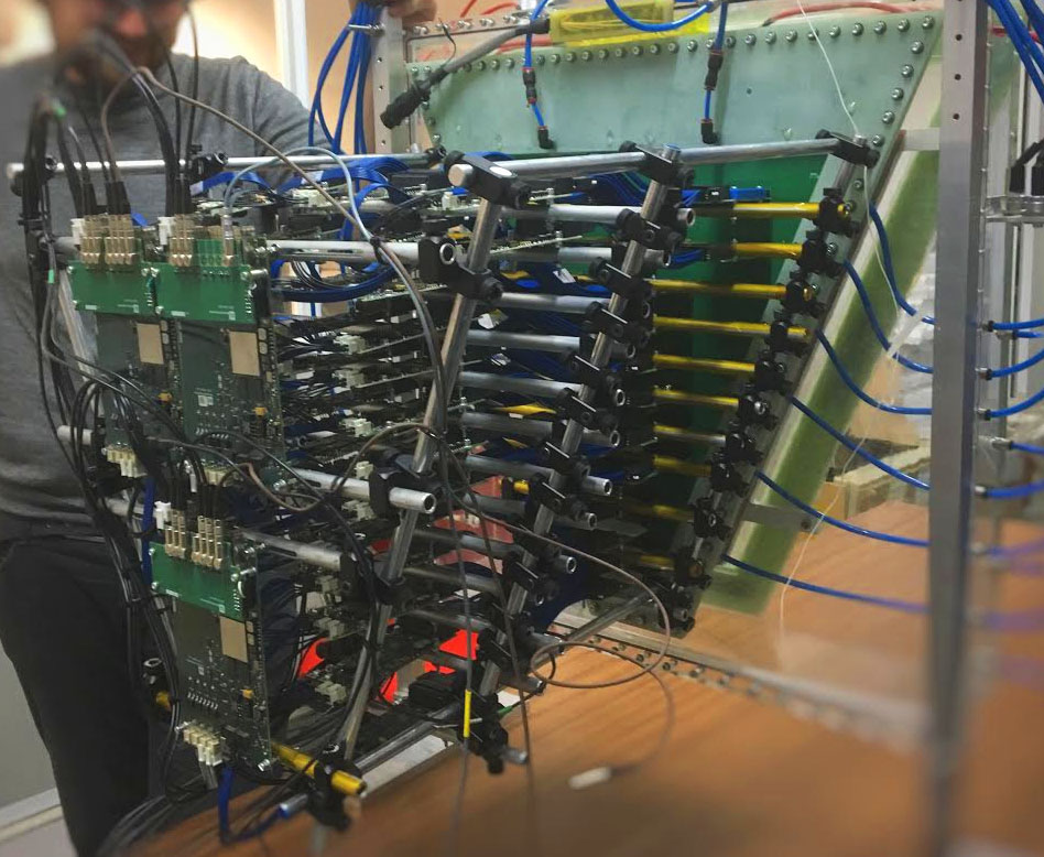
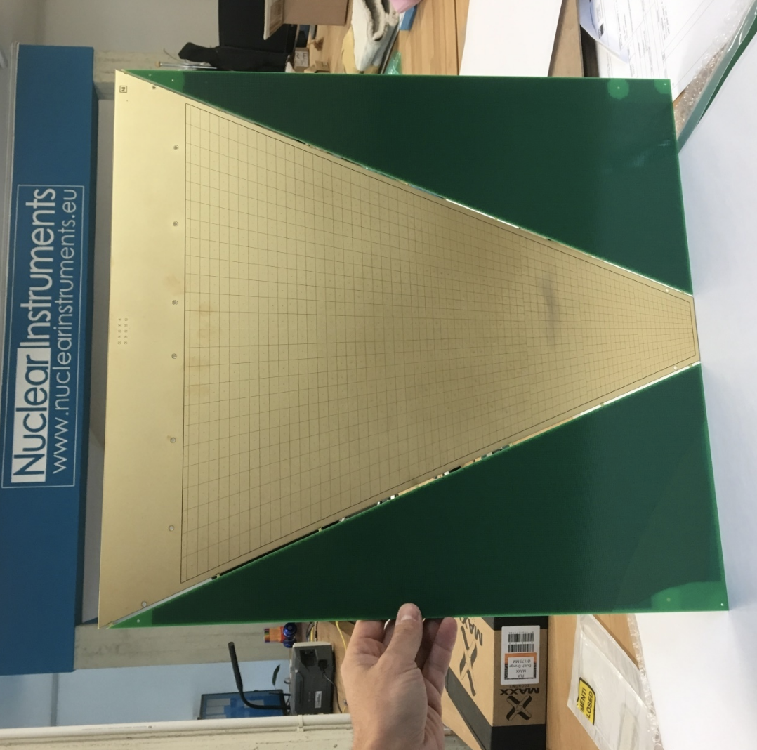
Example Application: